- 您现在的位置:买卖IC网 > Sheet目录1214 > EVAL-ADM1075CEBZ (Analog Devices Inc)BOARD EVAL FOR ADM1075
�� �
�
�V� TIMERH� � C� TIMER� (� V� TIMERH� /� V� TIMERL� )� � C� TIMER�
�t� INITIAL� =� +�
�ADM1075�
�timing� cycle.� The� TIMER� pin� is� pulled� up� with� 3� μA.� When� the�
�TIMER� reaches� the� V� TIMERH� threshold� (1.0� V),� the� first� portion�
�of� the� initial� cycle� is� complete.� The� 100� μA� current� source� then�
�pulls� down� the� TIMER� pin� until� it� reaches� V� TIMERL� (0.05� V).� The�
�initial� cycle� duration� is� related� to� C� TIMER� by� the� following� equation:�
�3� μA� 100� μA�
�For� example,� a� 470� nF� capacitor� results� in� a� power-up� delay� of�
�approximately� 160� ms.� Provided� the� UV� and� OV� detectors� are�
�inactive� when� the� initial� timing� cycle� terminates,� the� device� is�
�ready� to� start� a� hot� swap� operation.�
�When� the� voltage� across� the� sense� resistor� reaches� the� circuit�
�breaker� trip� voltage,� V� CB� ,� the� 60� μA� timer� pull-up� current� is�
�activated,� and� the� gate� begins� to� regulate� the� current� at� the� current�
�Data� Sheet�
�advantage� of� setting� very� low� inrush� currents� where� required� by�
�combination� of� large� output� capacitance� and� FET� SOA� limitations.�
�The� object� of� such� a� design� is� to� allow� a� linear� monotonic�
�power-up� event� without� the� restrictions� of� the� system� fault�
�timer.� To� achieve� this,� a� power-up� ramp� is� set� so� that� the� inrush�
�is� low� enough� not� to� reach� the� circuit� breaker� current� limit,� or�
�constant� power� current� limit.� This� allows� power-up� to� continue�
�without� the� timer� running.� When� using� this� method,� take�
�separate� care� to� ensure� the� power� in� the� MOSFET� during� this�
�event� meets� the� SOA� requirements.� The� components� labeled�
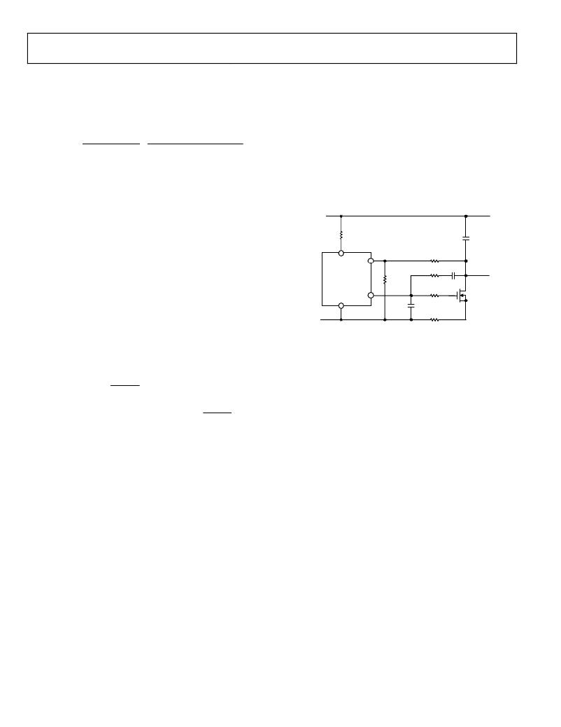
�R� GD� ,� C� GD� and� C� G� on� the� gate� pin� in� Figure� 51� show� the� required�
�extra� components.�
�0V�
�C� LOAD�
�PLIM�
�limit.� This� initiates� a� ramp-up� on� the� TIMER� pin.� If� the� sense�
�voltage� falls� below� this� circuit� breaker� trip� voltage� before� the�
�TIMER� pin� reaches� V� TIMERH� (1.0� V),� the� 60� μA� pull-up� is�
�disabled,� and� the� 2� μA� pull-down� is� enabled.�
�The� circuit� breaker� trip� voltage� is� not� the� same� as� the� hot� swap�
�sense� voltage� current� limit.� There� is� a� small� circuit� breaker�
�offset,� V� CBOS� ,� which� means� that� the� timer� actually� starts� a� short�
�–48V�
�VIN�
�ADM1075�
�GATE�
�VEE�
�R� PLIM2�
�C� G�
�R� PLIM1�
�R� GD�
�1� 0?�
�R� SENSE�
�C� GD�
�D�
�S�
�time� before� the� current� reaches� the� defined� current� limit.�
�However,� if� the� overcurrent� condition� is� continuous� and� the�
�sense� voltage� remains� above� the� circuit� breaker� trip� voltage,� the�
�60� μA� pull-up� remains� active� and� the� FET� remains� in� regulation.�
�This� allows� the� TIMER� pin� to� reach� V� TIMERH� and� initiate� the�
�GATE� shutdown.� The� LATCH� pin� is� pulled� low� immediately.�
�In� latch-off� mode,� the� TIMER� pin� is� switched� to� t� he 2 μA� pull-�
�down� when� it� reaches� the� V� TIMERH� threshold.� The� LATCH� pin�
�remains� low.� While� the� TIMER� pin� is� being� pulled� down,� the�
�hot� swap� controller� is� kept� off� and� cannot� be� turned� back� on.�
�When� the� voltage� on� the� TIMER� pin� goes� below� the� V� TIMERL�
�threshold,� the� hot� swap� controller� can� be� reenabled� by� toggling�
�the� UVx� pin� or� by� using� the� PMBus� OPERATION� command� to�
�toggle� the� ON� bit� from� on� to� off� and� then� on� again.�
�SETTING� A� LINEAR� OUTPUT� VOLTAGE� RAMP� AT�
�POWER-UP�
�The� ADM1075� standard� method� of� operation� is� to� control� a� constant�
�power� in� the� MOSFET� during� power-up� into� the� load.� This� can�
�result� in� non-linear� output� voltage� ramps� and� often� requires�
�many� retry� attempts� to� charge� larger� load� capacitances,� due� to�
�MOSFET� SOA� limitations.� However,� there� is� a� way� to� configure�
�a� single� linear� voltage� ramp� on� the� output� which� allows� a� constant�
�inrush� current� to� be� maintained.� For� a� typical� power-up� using�
�constant� power,� as� the� output� voltage� increases� in� magnitude,�
�the� controlled� current� also� increases� to� maintain� a� constant� power�
�in� the� pass� MOSFET.� This� can� be� a� challenge� for� maintaining�
�MOSFET� SOA,� where� higher� drain� currents� limit� energy� transfer�
�Figure� 51.� Required� Extra� Components�
�To� ensure� the� inrush� current� does� not� approach� or� exceed� the�
�active� current� limit� level,� the� output� voltage� ramp� can� be� set� by�
�selecting� the� appropriate� value� for� C� GD� as� follows:�
�C� GD� =� (� I� GATEUP� /� I� INRUSH� )� � C� LOAD�
�where� I� GATEUP� is� the� gate� pull-up� current� specified.�
�Add� margin� and� tolerance� as� necessary� to� ensure� a� robust�
�design.� Subtract� any� parasitic� C� GD� of� the� MOSFETS� from� the�
�total� to� determine� the� additional� external� capacitance� required.�
�The� power-up� ramp� time� can� now� be� approximated� by:�
�t� RAMP� =� (V� IN� � C� LOAD� )/I� INRUSH�
�Check� the� SOA� of� the� MOSFET� for� conditions� and� the� duration�
�of� this� power-up� ramp.�
�R� GD� and� C� G� are� used� to� limit� the� impact� of� sudden� transients� on�
�the� MOSFET� Drain� pin� being� coupled� to� the� GATE� pin� through�
�C� GD� .� R� G� is� chosen� such� that� I� GATEUP� has� minimal� voltage� drop�
�impact.� Typical� values� would� be� 1� K.� As� a� rule,� C� G� is� recommended�
�to� be� about� 10� the� value� of� C� GD� ,� to� a� maximum� of� 470� nF.� C� G�
�must� be� minimized� and� must� not� exceed� 470� nF� to� avoid� slowing�
�down� gate� shutdown� in� response� to� severe� overcurrent� events.�
�This� capacitance� results� in� slowing� down� the� gate� ramp� through�
�V� TH� and� therefore� the� trans-conductance� current� ramp.� This�
�delay� must� also� be� considered� when� checking� SOA� during�
�power-up� into� a� fault.� When� using� this� method,� always� remove�
�the� SS� cap,� and� TIMER� can� be� minimized� to� provide� a� simple�
�fault� filtering� solution.�
�more� than� lower� currents.� However,� if� the� output� voltage� is�
�programmed� to� result� in� a� linear� ramp,� the� inrush� into� the� load�
�capacitance� remains� somewhat� constant.� This� can� have� the�
�Rev.� C� |� Page� 24� of� 52�
�发布紧急采购,3分钟左右您将得到回复。
相关PDF资料
EVAL-ADM1087EBZ
BOARD EVALUATION FOR ADM1087
EVAL-ADM1166TQEBZ
BOARD EVAL FOR ADM1166TQ
EVAL-ADM1168LQEBZ
BOARD EVAL FOR ADM1168LQ
EVAL-ADM1170EBZ
BOARD EVALUATION FOR ADM1170
EVAL-ADM1171EBZ
BOARD EVALUATION FOR ADM1171
EVAL-ADM1172EBZ
BOARD EVALUATION FOR ADM1172
EVAL-ADM1175EBZ
BOARD EVALUATION FOR ADM1175
EVAL-ADM1176EBZ
BOARD EVALUATION FOR ADM1176
相关代理商/技术参数
EVAL-ADM1075EBZ
制造商:Analog Devices 功能描述:EVAL -48V CONTROLLER ADM1075 制造商:Analog Devices 功能描述:ADM1075, HOT SWAP, 350W, EVAL BOARD
EVAL-ADM1087EB
功能描述:BOARD EVAL FOR ADM1087 RoHS:否 类别:编程器,开发系统 >> 评估演示板和套件 系列:Simple Sequencers® 标准包装:1 系列:PSoC® 主要目的:电源管理,热管理 嵌入式:- 已用 IC / 零件:- 主要属性:- 次要属性:- 已供物品:板,CD,电源
EVAL-ADM1087EBZ
功能描述:BOARD EVALUATION FOR ADM1087 RoHS:是 类别:编程器,开发系统 >> 评估演示板和套件 系列:Simple Sequencers® 标准包装:1 系列:PSoC® 主要目的:电源管理,热管理 嵌入式:- 已用 IC / 零件:- 主要属性:- 次要属性:- 已供物品:板,CD,电源
EVAL-ADM1166TQEBZ
功能描述:BOARD EVAL FOR ADM1166TQ RoHS:是 类别:编程器,开发系统 >> 评估演示板和套件 系列:* 标准包装:1 系列:- 主要目的:电信,线路接口单元(LIU) 嵌入式:- 已用 IC / 零件:IDT82V2081 主要属性:T1/J1/E1 LIU 次要属性:- 已供物品:板,电源,线缆,CD 其它名称:82EBV2081
EVAL-ADM1168LQEBZ
功能描述:BOARD EVAL FOR ADM1168LQ RoHS:是 类别:编程器,开发系统 >> 评估演示板和套件 系列:* 标准包装:1 系列:- 主要目的:电信,线路接口单元(LIU) 嵌入式:- 已用 IC / 零件:IDT82V2081 主要属性:T1/J1/E1 LIU 次要属性:- 已供物品:板,电源,线缆,CD 其它名称:82EBV2081
EVAL-ADM1169LQEBZ
功能描述:BOARD EVAL FOR ADM1169LQ RoHS:是 类别:编程器,开发系统 >> 评估演示板和套件 系列:Super Sequencer® 标准包装:1 系列:PSoC® 主要目的:电源管理,热管理 嵌入式:- 已用 IC / 零件:- 主要属性:- 次要属性:- 已供物品:板,CD,电源
EVAL-ADM1170EBZ
功能描述:BOARD EVALUATION FOR ADM1170 RoHS:是 类别:编程器,开发系统 >> 评估演示板和套件 系列:- 标准包装:1 系列:- 主要目的:电信,线路接口单元(LIU) 嵌入式:- 已用 IC / 零件:IDT82V2081 主要属性:T1/J1/E1 LIU 次要属性:- 已供物品:板,电源,线缆,CD 其它名称:82EBV2081
EVAL-ADM1171EBZ
功能描述:BOARD EVALUATION FOR ADM1171 RoHS:是 类别:编程器,开发系统 >> 评估演示板和套件 系列:- 标准包装:1 系列:- 主要目的:电信,线路接口单元(LIU) 嵌入式:- 已用 IC / 零件:IDT82V2081 主要属性:T1/J1/E1 LIU 次要属性:- 已供物品:板,电源,线缆,CD 其它名称:82EBV2081